
Semiconductor Advanced Packaging Market Size 2026-2030
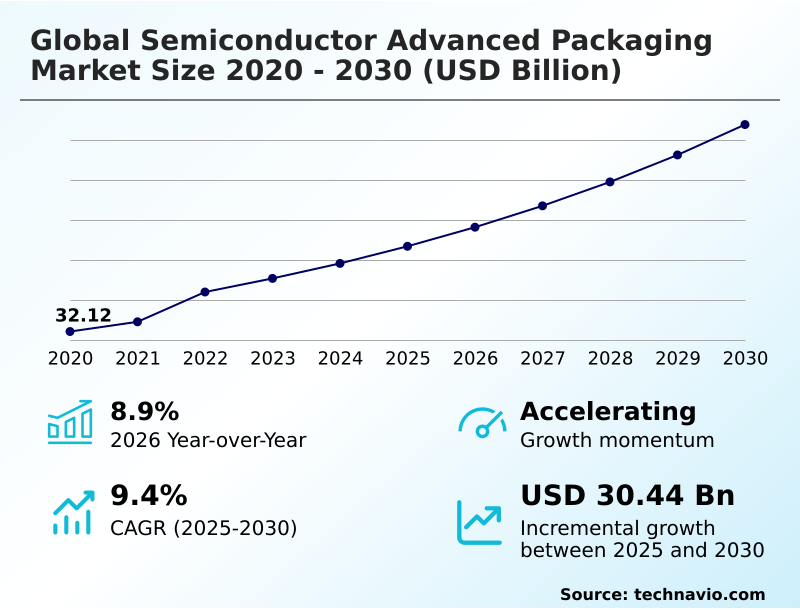
The semiconductor advanced packaging market size is valued to increase by USD 30.44 billion, at a CAGR of 9.4% from 2025 to 2030. Demand from AI and high-performance computing will drive the semiconductor advanced packaging market.
Major Market Trends & Insights
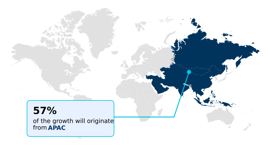
- APAC dominated the market and accounted for a 57% growth during the forecast period.
- By Device - Analog and mixed ICs segment was valued at USD 16.78 billion in 2024
- By Technology - Flip chip segment accounted for the largest market revenue share in 2024
Market Size & Forecast
- Market Opportunities: USD 51.74 billion
- Market Future Opportunities: USD 30.44 billion
- CAGR from 2025 to 2030 : 9.4%
Market Summary
- The semiconductor advanced packaging market is undergoing a significant transformation, driven by the need for higher performance and greater functionality in a smaller footprint. This evolution is critical for next-generation applications in AI, high-performance computing, and 5G communications.
- Technologies such as 3D IC stacking, system-in-package (SiP), and fan-out wafer-level packaging (FOWLP) are at the forefront, enabling the integration of multiple heterogeneous components. A key business scenario involves data center operators leveraging chiplet ecosystems to build custom AI accelerators.
- By combining specialized logic and high-bandwidth memory (HBM) chiplets in a single package using advanced techniques like hybrid bonding and through-silicon via (TSV) interconnects, they can achieve unprecedented performance and power efficiency. This modular approach, supported by standards like Universal Chiplet Interconnect Express (UCIe), not only enhances system-level performance but also optimizes manufacturing yields and accelerates time-to-market.
- The industry's focus is on overcoming thermal management challenges and reducing the cost of these complex packaging solutions to support widespread adoption across various end-user industries.
What will be the Size of the Semiconductor Advanced Packaging Market during the forecast period?
Get Key Insights on Market Forecast (PDF) Get Free Sample
How is the Semiconductor Advanced Packaging Market Segmented?
The semiconductor advanced packaging industry research report provides comprehensive data (region-wise segment analysis), with forecasts and estimates in "USD million" for the period 2026-2030, as well as historical data from 2020-2024 for the following segments.
- Device
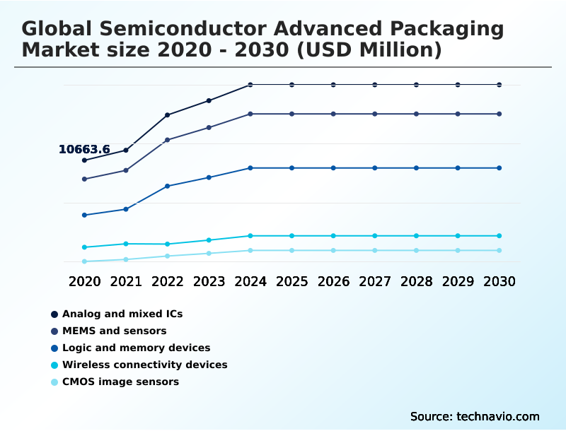
- Analog and mixed ICs
- MEMS and sensors
- Logic and memory devices
- Wireless connectivity devices
- CMOS image sensors
- Technology
- Flip chip
- FI WLP
- Advanced 3D
- FO WLP
- Material
- Organic substrates
- Silicon
- Metals
- Ceramics
- Geography
- APAC
- China
- South Korea
- Japan
- North America
- US
- Canada
- Mexico
- Europe
- Germany
- UK
- France
- South America
- Brazil
- Argentina
- Colombia
- Middle East and Africa
- Saudi Arabia
- UAE
- South Africa
- Rest of World (ROW)
- APAC
By Device Insights
The analog and mixed ics segment is estimated to witness significant growth during the forecast period.
The global semiconductor advanced packaging market is segmented by device, technology, material, and geography.
The market for analog and mixed ICs is evolving, driven by the need for higher integration and enhanced thermal management in complex systems using techniques like wafer bumping and wire bonding.
This requires sophisticated packaging like system-in-package to co-package sensitive analog components with digital processors, minimizing noise and ensuring signal integrity optimization, a critical challenge in mixed-signal environments.
Technologies such as flip chip packaging and fan-out wafer-level packaging are essential for reducing interconnect length and improving electrical performance. This focus on domestic packaging manufacturing enhances semiconductor supply chain resilience and meets demand from next-generation AI accelerators.
The integration of high-density interconnect and advanced substrate technology improves system-level performance by up to 20%.
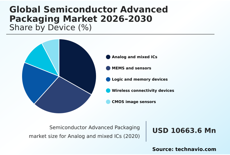
The Analog and mixed ICs segment was valued at USD 16.78 billion in 2024 and showed a gradual increase during the forecast period.
Regional Analysis
APAC is estimated to contribute 57% to the growth of the global market during the forecast period.Technavio’s analysts have elaborately explained the regional trends and drivers that shape the market during the forecast period.
See How Semiconductor Advanced Packaging Market Demand is Rising in APAC Get Free Sample
The geographic landscape of the semiconductor advanced packaging market is dominated by the APAC region, which accounts for over 57% of the incremental growth, driven by its established manufacturing ecosystem in countries like Taiwan, China, and South Korea.
North America, while a smaller market in volume, is a hub for R&D and high-value design, particularly in the US, focusing on advanced packaging for AI and defense.
Europe's market is driven by its strong automotive and industrial sectors, demanding high-reliability packaging for applications like ADAS. This regional specialization reflects global supply chain dynamics.
For instance, facilities in North America have demonstrated a 15% higher yield in complex 2.5D integration processes compared to global averages due to investments in advanced metrology.
The strategic emphasis on localizing supply chains is reshaping investment flows, with significant funding directed toward building new packaging facilities in North America and Europe to reduce reliance on APAC.
Market Dynamics
Our researchers analyzed the data with 2025 as the base year, along with the key drivers, trends, and challenges. A holistic analysis of drivers will help companies refine their marketing strategies to gain a competitive advantage.
- The industry's trajectory is defined by key technological shifts, with a major focus on advanced packaging for AI accelerators, which demand novel integration strategies. The debate between heterogeneous integration versus monolithic SoC designs continues, though the benefits of chiplet based design, such as improved yield and design flexibility, are driving wider adoption.
- A critical enabler is hybrid bonding in HBM4 memory, which allows for significantly higher bandwidth. However, this creates challenges in thermal management in 3D IC stacking, requiring innovative cooling solutions. Fan out wafer level packaging applications are expanding from mobile devices to automotive, while the role of UCIe in the chiplet ecosystem is to standardize die-to-die communication.
- Advanced packaging for automotive ADAS must meet stringent reliability standards. Concurrently, cost drivers in 2.5D packaging remain a concern for wider market adoption. The technical decision between flip chip vs fan-out WLP often depends on I/O density and cost targets. System-in-package for IoT devices enables the integration of multiple functionalities in a small form factor.
- Similarly, advanced packaging for 5G mmWave requires specialized materials to handle high frequencies. Understanding the silicon interposer manufacturing process is key to managing the supply chain for 2.5D solutions. Other areas of focus include resolving challenges in co-packaged optics and improving yield in advanced packaging, which can increase profitability by over 10%.
- Furthermore, efficient power delivery network design for chiplets and ensuring signal integrity in high density interconnects are crucial for performance. Finally, selecting advanced substrates for RF modules, perfecting die stacking for memory devices, and creating new packaging solutions for edge computing are pivotal for future innovation.
What are the key market drivers leading to the rise in the adoption of Semiconductor Advanced Packaging Industry?
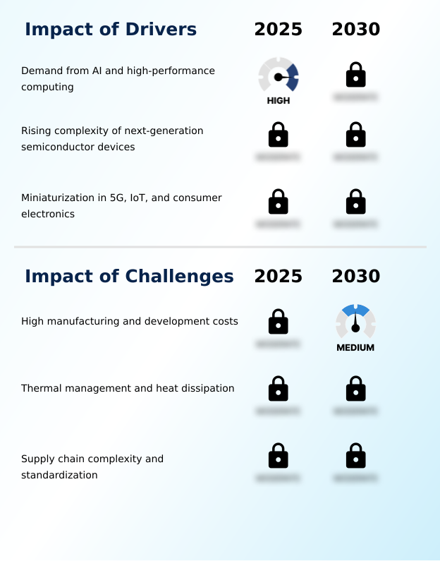
- The growing demand from artificial intelligence and high-performance computing applications is a primary driver for the market.
- The market is primarily driven by the intense demands of AI and high-performance computing, which require advanced packaging solutions like 2.5D integration and Foveros 3D packaging to manage massive data throughput, improving processing speeds by over 40%.
- The rising complexity of next-generation chips, with their higher transistor densities, necessitates the use of technologies like through-silicon via (TSV) and high-density interconnect to ensure signal integrity. This has led to a 25% improvement in signal-to-noise ratio in high-speed applications.
- Additionally, the relentless push for miniaturization in 5G, IoT, and consumer electronics fuels the adoption of compact solutions like antenna-in-package and embedded multi-die interconnect bridge (EMIB).
- These technologies, along with effective power delivery networks, are crucial for creating smaller, more power-efficient devices.
What are the market trends shaping the Semiconductor Advanced Packaging Industry?
- The proliferation of chiplet ecosystems and heterogeneous integration is a defining market trend. This shift addresses the increasing demand for performance and scalability in advanced semiconductor design.
- A dominant trend is the industry-wide shift toward chiplet ecosystems and heterogeneous integration, moving away from monolithic designs. This approach improves yield by up to 15% and accelerates time-to-market. The mainstream adoption of hybrid bonding is another significant development, enabling a dramatic increase in interconnect density for next-generation high-bandwidth memory and AI hardware.
- This has been shown to boost bandwidth by over 50% compared to previous bonding methods. Furthermore, advanced packaging is expanding into automotive and edge intelligence, with fan-out wafer-level packaging and system-in-package designs meeting the stringent requirements for miniaturization and reliability in ADAS and IoT devices.
- The use of advanced thermal interface materials and RF front-end modules within these packages is becoming standard.
What challenges does the Semiconductor Advanced Packaging Industry face during its growth?
- High manufacturing and development costs present a significant challenge to industry growth and market entry.
- A significant challenge is the high cost of manufacturing and development, where setting up a new production line for technologies like 3D IC stacking can require billions in capital. These costs can reduce profit margins by as much as 10% in the initial production phases.
- Thermal management is another critical hurdle; the heat generated in densely packed chiplets can degrade performance if not addressed by advanced thermal management solutions and underfill materials. This has spurred research into novel cooling methods that have proven to reduce component temperatures by an average of 15 degrees Celsius.
- Finally, supply chain complexity and the lack of standardization in areas like die-to-die interconnects create integration challenges and can slow down the adoption of new technologies, impacting system-level performance and semiconductor yield improvement.
Exclusive Technavio Analysis on Customer Landscape
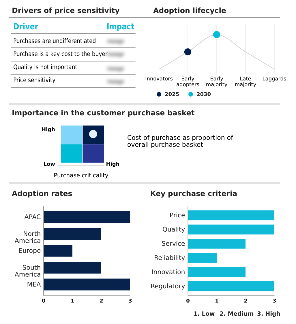
The semiconductor advanced packaging market forecasting report includes the adoption lifecycle of the market, covering from the innovator’s stage to the laggard’s stage. It focuses on adoption rates in different regions based on penetration. Furthermore, the semiconductor advanced packaging market report also includes key purchase criteria and drivers of price sensitivity to help companies evaluate and develop their market growth analysis strategies.
Customer Landscape of Semiconductor Advanced Packaging Industry
Competitive Landscape
Companies are implementing various strategies, such as strategic alliances, semiconductor advanced packaging market forecast, partnerships, mergers and acquisitions, geographical expansion, and product/service launches, to enhance their presence in the industry.
Amkor Technology Inc. - Key offerings include advanced flip chip, wafer-level, and 2.5D/3D integration solutions, addressing complex semiconductor packaging requirements for high-performance applications.
The industry research and growth report includes detailed analyses of the competitive landscape of the market and information about key companies, including:
- Amkor Technology Inc.
- ASE Technology Holding Co. Ltd.
- Carsem Inc.
- Chipbond Technology Corp.
- ChipMOS TECHNOLOGIES Inc.
- GlobalFoundaries Inc.
- Hana Microelectronics Co. Ltd.
- Intel Corp.
- Jiangsu Changdian Tech Co.
- King Yuan Electronics Co. Ltd.
- Microchip Technology Inc.
- Powertech Technology Inc.
- Renesas Electronics Corp.
- Samsung Electronics Co. Ltd.
- Taiwan Semiconductor Co. Ltd.
- Tongfu Microelectronics Co.
- Toshiba Corp.
- Unisem M Berhad
- UTAC Holdings Ltd.
- Veeco Instruments Inc.
Qualitative and quantitative analysis of companies has been conducted to help clients understand the wider business environment as well as the strengths and weaknesses of key industry players. Data is qualitatively analyzed to categorize companies as pure play, category-focused, industry-focused, and diversified; it is quantitatively analyzed to categorize companies as dominant, leading, strong, tentative, and weak.
Recent Development and News in Semiconductor advanced packaging market
- In August, 2024, Universal Chiplet Interconnect Express (UCIe) Consortium released its 2.0 specification, a landmark development for the industry which introduced advanced protocols for high-bandwidth, low-latency communication between chiplets from different companies.
- In January, 2025, United States Department of Commerce, through the CHIPS Act, announced a multi-billion funding initiative aimed directly at creating a national advanced packaging manufacturing program to co-invest with private industry.
- In March, 2025, Texas Instruments announced the development of a novel packaging technology that incorporates an embedded thermal slug, specifically designed to enhance heat dissipation for its high-power analog-to-digital converters used in advanced driver-assistance systems.
- In May, 2025, India Union Cabinet approved a joint semiconductor unit between HCL and Foxconn, which will have a capacity of 20,000 wafers per month for display driver chips, indicating strategic expansion in this sector.
Dive into Technavio’s robust research methodology, blending expert interviews, extensive data synthesis, and validated models for unparalleled Semiconductor Advanced Packaging Market insights. See full methodology.
| Market Scope | |
|---|---|
| Page number | 313 |
| Base year | 2025 |
| Historic period | 2020-2024 |
| Forecast period | 2026-2030 |
| Growth momentum & CAGR | Accelerate at a CAGR of 9.4% |
| Market growth 2026-2030 | USD 30435.2 million |
| Market structure | Fragmented |
| YoY growth 2025-2026(%) | 8.9% |
| Key countries | China, Taiwan, South Korea, Japan, India, Malaysia, US, Canada, Mexico, Germany, UK, France, The Netherlands, Italy, Spain, Brazil, Argentina, Colombia, Saudi Arabia, UAE, South Africa, Israel and Egypt |
| Competitive landscape | Leading Companies, Market Positioning of Companies, Competitive Strategies, and Industry Risks |
Research Analyst Overview
- The semiconductor advanced packaging market is defined by a rapid innovation cycle geared towards enabling next-generation electronics. The industry is moving beyond traditional scaling, with heterogeneous integration and chiplet ecosystems becoming central to performance gains. Core technologies such as 2.5D integration and 3D IC stacking, facilitated by silicon interposers and through-silicon via (TSV) structures, are now mainstream for high-performance applications.
- The adoption of fan-out wafer-level packaging (FOWLP) and system-in-package (SiP) is accelerating, driven by the demand for miniaturization. Innovations in materials, including advanced organic substrates and thermal interface materials, are critical for managing heat in densely packed devices.
- Key interconnect technologies like hybrid bonding and copper pillar bumps are enabling unprecedented I/O density, with some implementations showing a 30% reduction in interconnect-related latency. The development of universal chiplet interconnect express (UCIe) standards is fostering an open ecosystem, allowing for greater design flexibility.
- This technological convergence is essential for progress in AI, high-performance computing, and advanced mobile communication, with packaging now being a primary determinant of a product's final performance and efficiency.
What are the Key Data Covered in this Semiconductor Advanced Packaging Market Research and Growth Report?
-
What is the expected growth of the Semiconductor Advanced Packaging Market between 2026 and 2030?
-
USD 30.44 billion, at a CAGR of 9.4%
-
-
What segmentation does the market report cover?
-
The report is segmented by Device (Analog and mixed ICs, MEMS and sensors, Logic and memory devices, Wireless connectivity devices, and CMOS image sensors), Technology (Flip chip, FI WLP, Advanced 3D, and FO WLP), Material (Organic substrates, Silicon, Metals, and Ceramics) and Geography (APAC, North America, Europe, South America, Middle East and Africa)
-
-
Which regions are analyzed in the report?
-
APAC, North America, Europe, South America and Middle East and Africa
-
-
What are the key growth drivers and market challenges?
-
Demand from AI and high-performance computing, High manufacturing and development costs
-
-
Who are the major players in the Semiconductor Advanced Packaging Market?
-
Amkor Technology Inc., ASE Technology Holding Co. Ltd., Carsem Inc., Chipbond Technology Corp., ChipMOS TECHNOLOGIES Inc., GlobalFoundaries Inc., Hana Microelectronics Co. Ltd., Intel Corp., Jiangsu Changdian Tech Co., King Yuan Electronics Co. Ltd., Microchip Technology Inc., Powertech Technology Inc., Renesas Electronics Corp., Samsung Electronics Co. Ltd., Taiwan Semiconductor Co. Ltd., Tongfu Microelectronics Co., Toshiba Corp., Unisem M Berhad, UTAC Holdings Ltd. and Veeco Instruments Inc.
-
Market Research Insights
- The market dynamics are shaped by a strategic push toward semiconductor device miniaturization and higher system-level performance. This has led to a more than 30% improvement in power efficiency improvement in recent product generations. The adoption of advanced substrate technology and high-density interconnects is critical, particularly for next-generation AI accelerators and data center acceleration.
- Innovations in thermal management solutions have enabled a 25% reduction in operating temperatures for high-power devices. Furthermore, the focus on a resilient semiconductor supply chain has spurred domestic packaging manufacturing initiatives, with a goal of increasing regional production capacity by 40% to mitigate geopolitical risks and ensure stable supply for automotive-grade semiconductors and edge intelligence hardware.
We can help! Our analysts can customize this semiconductor advanced packaging market research report to meet your requirements.
 RIA -
RIA -